
Abstract: This paper summarizes the research status of new fields in the combination of laser technology and electroplating and electroless plating. Respectively, introduced the early work, recent research results and future development direction. This new technology is particularly suitable for microelectronics industry circuit design and repair and aerospace technology.
Keywords: laser plating, electroplating, microelectronics, new technology
In recent years, due to the miniaturization of electronic products and the rapid development of highly integrated, in the small part of the surface processing. Therefore, laser-enhanced electroplating and etching applied to the field of microelectronics in the local deposition or etching, has attracted more and more attention. In the liquid phase and gas phase can be used for laser surface treatment, a representative liquid phase laser surface treatment is laser plating and laser etching. When a continuous laser or pulsed laser is used to irradiate the cathode surface in the electrolytic cell, not only can the deposition rate of the metal be greatly increased, but also the computer can control the motion trajectory of the laser beam to obtain the desired complex geometries. Laser plating is developed in recent years, a high-speed electroplating new technology, has aroused widespread interest.
Laser is a very high energy density heat source, and has a good direction, monochromatic and coherence. Using these features, the metal or part of the surface to strengthen the treatment (including laser phase transformation hardening laser alloying and laser cladding, etc.) can change the metal or parts of the surface microstructure, improve the parts of the anti-wear, corrosion resistance and fatigue resistance Laser processing of high precision, energy concentration, the impact of small parts of the small.
Electroplating and electroless plating as the traditional surface technology after a long period of development, the process has been very mature. Researchers have combined laser and traditional surface technology to make a lot of research into this cross field.
Conventional plating is carried out between two electrodes immersed in the electrolyte, the metal substrate to be plated is placed in a salt solution containing a metal, driven by an external power source and subjected to electrolytic action to reduce the deposition of metal ions on the surface of the substrate Into a metal coating. Further research shows that the ion transport process mainly has the diffusion, convection and electromigration in three ways, to improve the rate of these three methods can take the following measures
(1) to improve the temperature of the electrolyte,
(2) stirring the electrolyte,
(3) Increase the inter-pole voltage or reduce the polar distance,
(4) increase the concentration of electroplating solution.
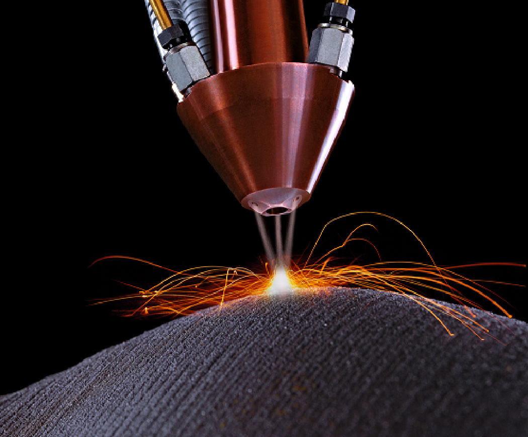
The basic principle of laser plating can be summarized as follows: the cathode absorbs the laser energy and causes the photo-induced temperature to rise, resulting in the local area of the electrochemical reaction greatly enhanced, resulting in the cathode surface by the light area deposition process of severe acceleration. This theoretical explanation of the laser-induced electroplating enhancement effect is called the thermal model of laser plating. There is also an optical model to explain the effect of plating enhancement, which suggests that the enhancement of the plating reaction is due to the photolysis effect, that is, the laser promotes the increase of the electrochemical reaction rate caused by the electrolyte self-decomposition, resulting in the plating rate The increase.
Laser-enhanced electroplating is a high-density laser beam irradiation / solidification interface, resulting in local temperature rise and micro-zone mixing, so as to induce or enhance the chemical reaction of the irradiation area, causing the decomposition of the liquid material and the reaction on the solid surface Product. In 1978, the United States IBM first studied the laser plating, the application of 1.5W hydrogen ion laser or hydrogen ion laser, the laser beam after focusing on the tungsten cathode, the deposition rate of nickel than the laser beam increased by 600-1000 times The
At present, although the principle of laser plating, laser ablation, plasma laser deposition and laser injection and other aspects are still being studied, but its technology has been used. Laser plating features Compared with the traditional electroplating process, laser plating technology has the following characteristics:
1) a high degree of selectivity can be micro-local plating metal, metal wire width can reach 2um.
2) wide adaptability. The laser plating can be carried out not only on metal (Al, Fe), but also on a variety of semiconductors (Si, GaAs), insulator (ceramic, glass-ceramic, polyimide, polytetrafluoroethylene) Au, Ag, Pd, Ni, Cu and the like.
3) high-speed deposition of laser induced deposition rate greatly improved, than conventional plating to a thousand times higher, such as gold plating when the deposition can be Au deposition rate of 30um / s.
4) can achieve computer control using computer-controlled laser beam scanning trajectory can be expected to a variety of line graphics.
5) the coating and the substrate have some mutual diffusion, the binding force is better than the general method.
6) can work at room temperature, simplify the process, save a lot of precious metals.
Laser plating is mainly based on the following two characteristics: ① in the laser irradiation area than the speed of the body plating much higher (about 103 times); ② laser control ability, can make the necessary part of the material precipitation The amount of metal required. Ordinary plating occurs on the entire electrode substrate, the plating speed is slow, it is difficult to form a complex and fine pattern. Laser plating can be used to adjust the laser beam to the size of the micron, in the size of the mask without masking. This type of high-speed tracing is becoming more and more practical for circuit design, circuit repair, and local deposition on microelectronic connector components.
Laser plating in addition to improve the plating rate, but also to improve the quality of the sedimentary layer. Laser irradiation can increase the rate of nucleation, so that the crystal particles small and dense. The thermal effect of the laser also acts as a local cleaning substrate surface, so that a tight coating can be obtained on a hard-laid substrate.
With the rapid development of microprocessors and microelectronics instrumentation, microelectronic components and large-scale integrated circuit board demand surged. Gold plating with its high heat resistance, high conductivity and easy welding and other excellent performance in the industry has been widely used. In this field, the traditional gold-plated production process is the use of shield re-plating or all the plating and then etching method. These processes are not only time consuming, but also waste a lot of expensive gold. People have been looking for a more economical gold-plated technology, laser-enhanced gold plating and came into being.
In order to improve the mass transfer, to further improve the plating speed, while the use of laser and liquid jet plating. For example, on a Be-Cu substrate, Au or Cu is sprayed with a laser-enhanced charge, with a gold plating rate of up to 10 um / s and a copper plating rate of up to 50 um / s.
Laser enhanced electroplating is an important research direction of laser chemical deposition, foreign countries have developed research, the United States, Germany and other countries, domestic research is still very little. Our experimental study on laser-enhanced electroplating is exploratory, but promising results have been achieved. We have been plated with a diameter of tens of microns of copper (or line), if the focus system to be improved, can be placed in the order of microns, the line. We have been coated with copper (line) samples for a long time (more than a month) test shows that: coating firmness is good. These two points for future microelectronic device fabrication and repair on the application is very valuable. At present, laser plating at home and abroad is in a continuous development stage, began for microelectronic circuits or electronic components manufacturing and repair, and promote the microelectronics instrumentation, aerospace, microcomputer and other industrial development.

Great development in plating process .how I can used it at my work shop .please confirm me .regards